Overview With ZITROK History
ZITROK ELECTRONICS CO., LIMITED is a professional company focusing on PCB & PCBA manufacture services.
We provide one-stop manufacture services of PCB & PCBA, including PCB production, material purchasing, SMT/PCBA, assembly test, etc.
We also provide complete and correct FAI test report, including the measurement of each material at
each position, abnormal material report and accurate judgment of design plan.
PCB Process Capability
We have a fully automatic plating and counterpart screen printing production line to provide high
high-quality PCB products to customers. In order to ensure the reliability of PCB, 10 sets of flying probe testers,
4 sets of test stand testers and high-accuracy FQC equipments are introduced.
| Layer |
1-24 |
| Dimension |
500 mm* 800 mm(2 layer); 400mm*550mm(multi-layer) |
| Thickness |
0.2mm-6.0mm |
| Copper |
Outer Layer 35um-420um, Inner Layer 17um-420um |
| Trace |
Minimum Trace Width/Space 0.075mm |
| Hole |
Minimum Hole Position Tolerance ±0.075mm |
| Surface Finish |
HASL, HASL Lead Free, OSP, ENIG, Immersion Tin, Immersion Silver and so on |
|
Impedance Control Tolerance
|
±10% |
| Test |
Open-Short Test, Solder Ability Test, Thermal Shock Test, Impedance Control Test |
Technology Cases
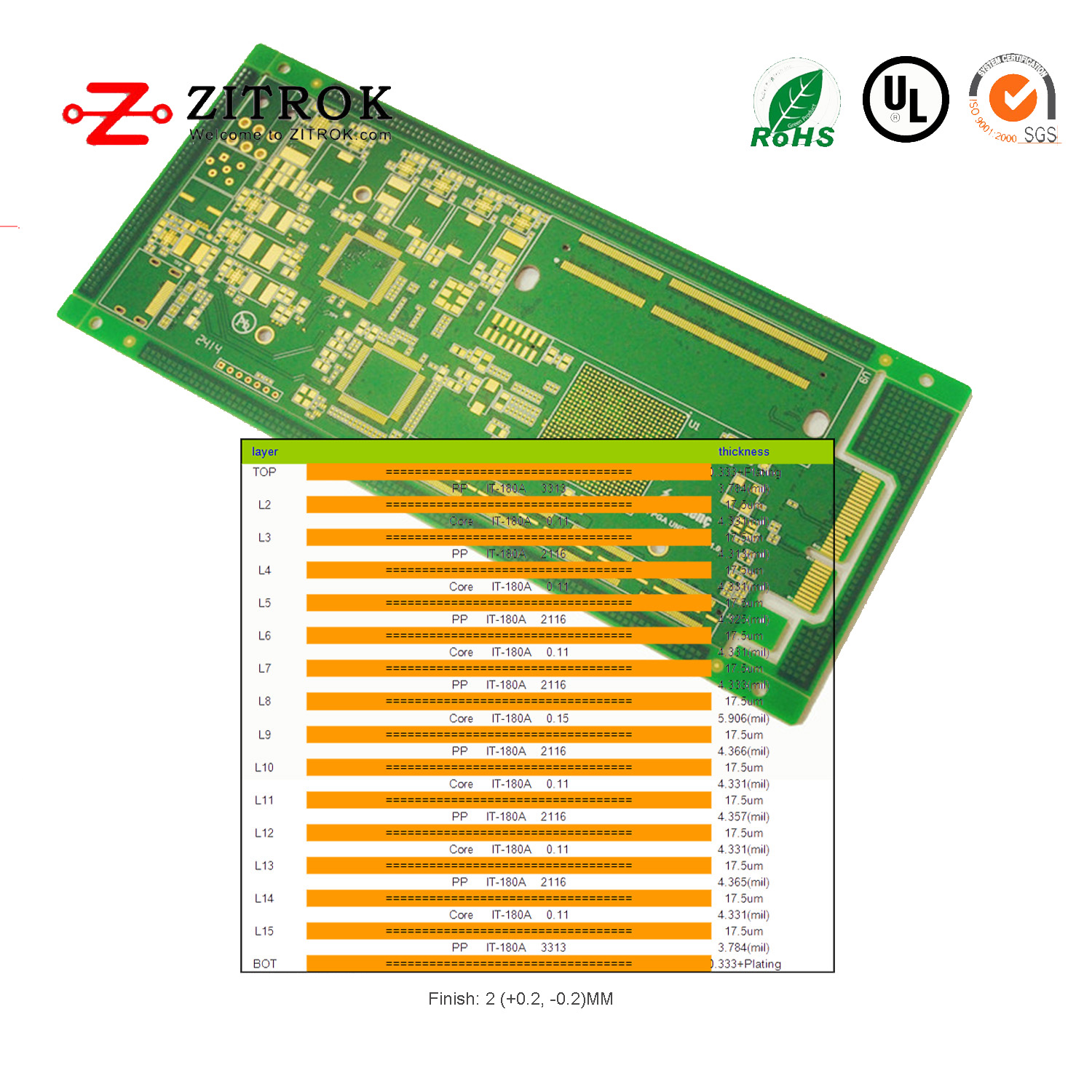
16 layers of High TG board-Internet of things
 Board material: High TG 170 FR4
Board thickness: 2.0mm
Number of layers: 16 layers
Size of single board: 194.33*87.56mm
Surface Finish: Immersion Gold
Copper thickness:2OZ
Wire width/space:5.9/5.9mil
Hole diameter:0.15mm
Impedance control tolerance: 10%
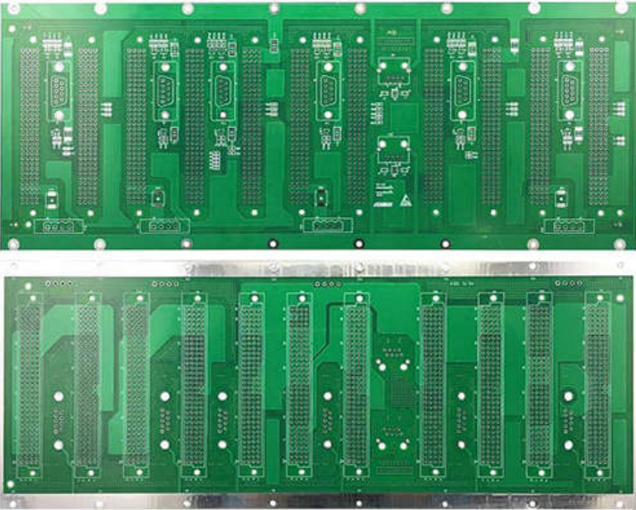
8 layers of PCB-smart transportation
 Board name:FS400053AAAB
Board material: ISOLA FR-370HR
Board thickness: 2.7mm
Number of layers:8
Size of single board: 336.05X 128.55mm
Surface treatment technology: Immersion Tin
Copper thickness:1OZ
Wire depth/distance:4.1/5mil
Hole diameter: 0.25mm

