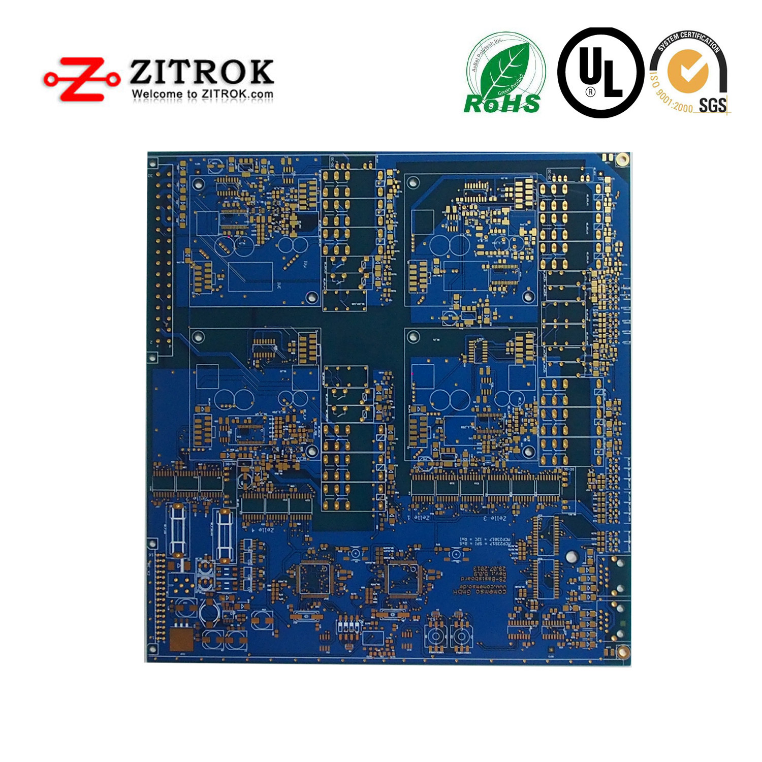
In order to improve the circuit density of electronic circuit boards and the require of the miniaturization and high integration of electronic products, so blind via and buried via technologies emerage. Before understanding what are blind vias and buried vias, let's first understand what is a via.
Via: A metalized hole used for inner layer connection. It is not used to insert component leads or other reinforcing materials.
Blind Vias: Blind vias connect the outermost circuit of the PCB with the adjacent inner layers with electroplated holes. Because the opposite side cannot be seen, it is called "blind through".
Buried Vias: Buried vias refer to the connection hole located in the inner layer of the printed circuit board, it will not extend to the surface of the circuit board.
Advantages Of Blind vias & Buried vias
(1)Greatly reducing the PCB size and reduce the number of layers, improving electromagnetic compatibility, and increasing the characteristics of electronic products.
In traditional PCB design and processing, vias will bring many problems. Firstly, they occupy a large amount of effective space, Secondly, a large number of vias are densely packed in one place, which also creates a huge obstacle to the inner layer wiring of the multilayer PCB. These vias occupy the space required for the wiring, and they intensively pass through the power supply and the ground. The surface of the wire layer will also destroy the impedance characteristics of the power ground wire layer and make the power ground wire layer ineffective.
(2) Improving The Reliability Of PCB
In PCB design, although the size of the pads and vias have gradually decreased, if the thickness of the board layer is not proportionally reduced, the aspect ratio of the via will increase, and the increase of the aspect ratio of the via will reduce the reliability. With the maturity of advanced laser drilling technology and plasma dry etching technology, it is possible to apply non-through small blind holes and small buried holes, which reduces the aspect ratio of the holes, thereby improving the reliability of the PCB.
(3)Improving EMI/RFI performance, Making the product more electrical performance
Due to the non-through via technology, there are few large vias on the PCB, which can provide more space for routing. The remaining space can be used for large-area shielding purposes, thereby improving EMI/RFI performance. At the same time, more remaining space can also be used for the inner layer to partially shield the device and key network cables, so that it has the best electrical performance. The use of non-through vias makes it easier to fan out the device pins, making it easy to route high-density pin devices (such as BGA package devices), shortening the wiring length, and meeting the timing requirements of high-speed circuits.
Technology Capacity Of Blind vias & Buried vias
| Via Type |
Via Diameter
(max.)
|
Via Diameter
(min.)
|
Via Pad |
Annular Ring |
Aspect Ratio |
| Blind via (mechanical) |
0.4mm |
150μm |
450μm |
127μm |
1:1 |
| Blind via (laser) |
0.1mm |
100μm |
254μm |
150μm |
1:1 |
| Buried via (mechanical) |
0.4mm |
100μm |
300μm |
150μm |
1:10 |
| Buried via (laser) |
0.4mm |
100μm |
225μm |
150μm |
1:12 |