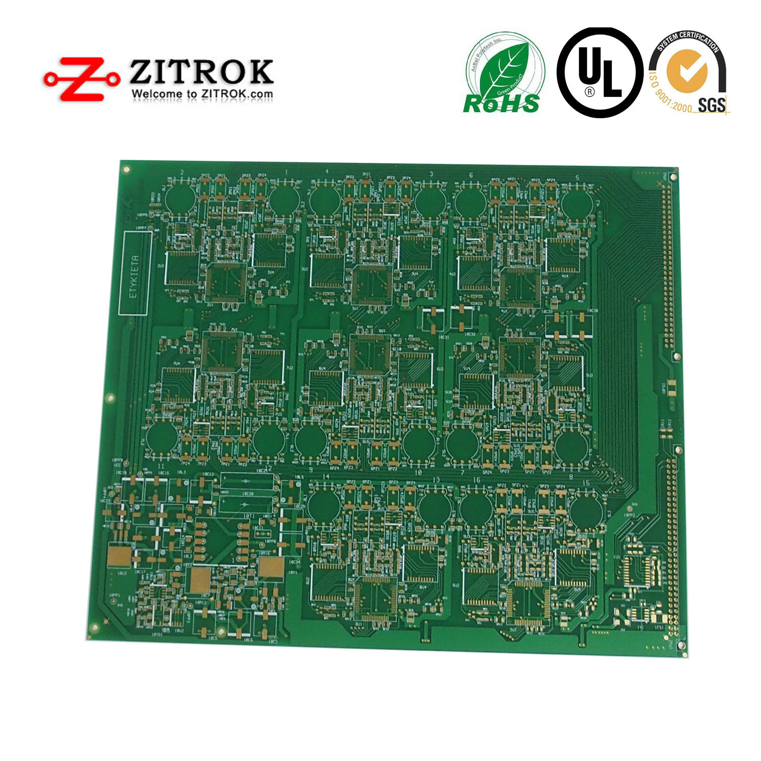
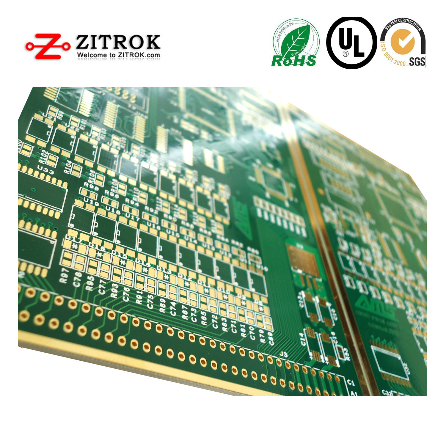
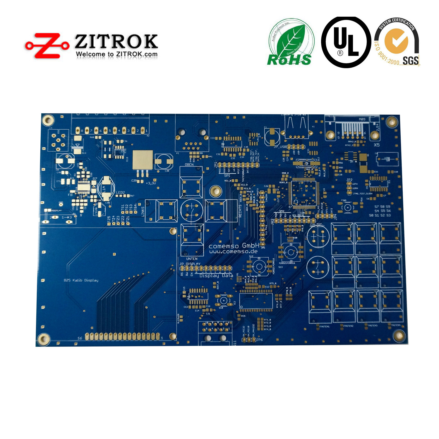
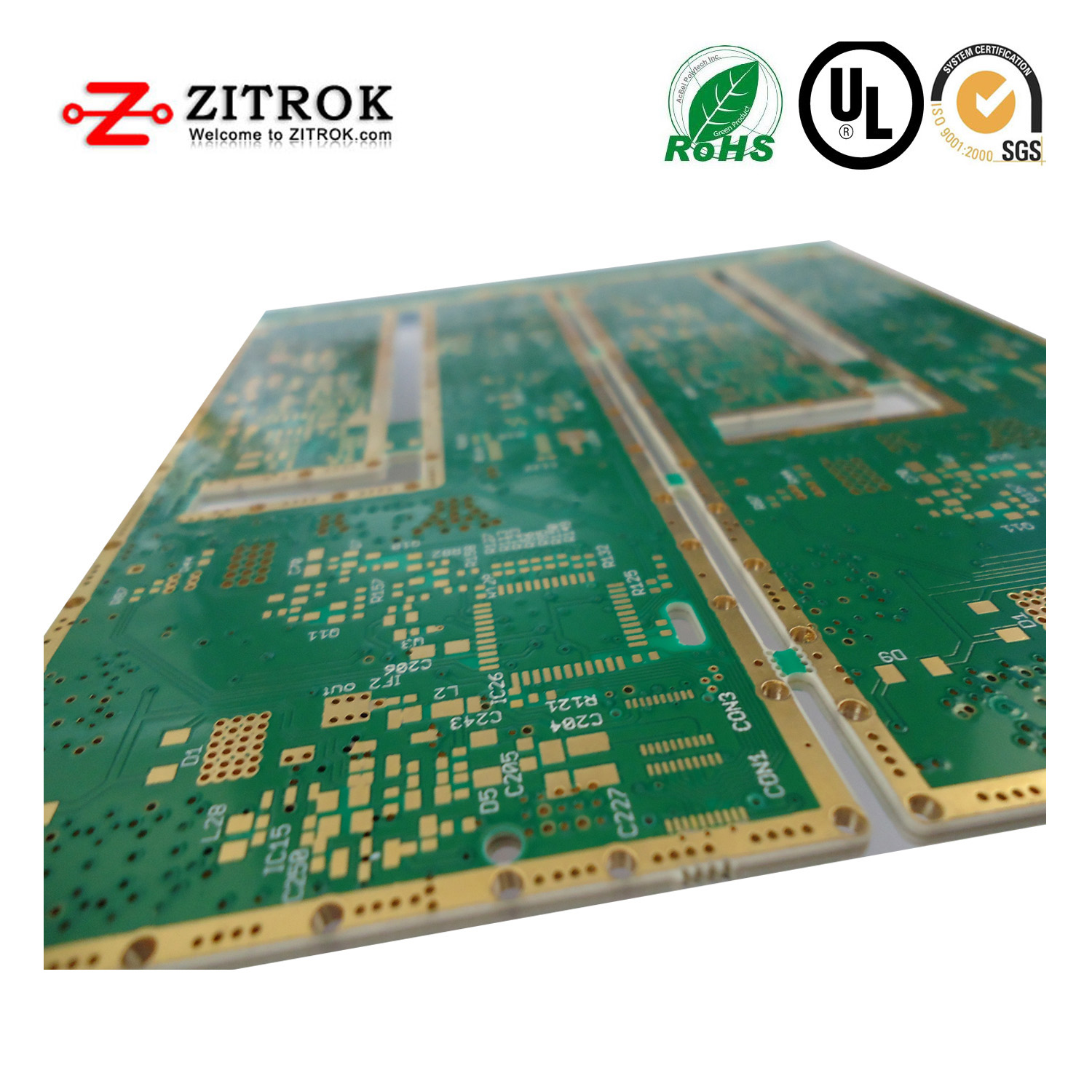
HDI also calles high-density interconnection board, which is a circuit board with relatively high line distribution density. Due to the high-density wiring, the medium between the wire layers is relatively thin, the diameter of the through hole is small, and the space occupied is small, which makes the signal transmission path in the wire short and fast, is very conducive to the transmission of high-frequency and high-speed signals. Compared with traditional PCB design techniques, HDI have finer lines and spacing, smaller through holes and pads, and higher connection pad density. HDI PCB is generally used to reduce PCB size and weight while meeting higher standards of electronic performance and efficiency.
HDI is a circuit board with a relatively high line distribution density that uses micro-blind and buried via technology to meet the needs of customers for smaller-sized complex designs in most market segments. HDI boards are generally manufactured by layer-by-layer method, the more the number of layers, the higher the technical level of the plate. Ordinary HDI boards are basically one-time build-up. High-end HDI uses two-time or more build-up technology. At the same time, advanced PCB technologies such as stacking holes, electroplating and filling holes, and laser direct drilling are used. When the density of the PCB increases beyond the eight-layer board, it is manufactured with HDI, and its cost is lower than the traditional complex pressing process.
Features Of HDI PCB Circuits
(1) Enable to reduce the pcb cost: while the density of PCB increases beyond eight-layer, the cost of using HDI will be more lower than traditional circuit boards.
(2)Having better electrical performance and signal accuracy.
(3)Can improve thermal properties.
(4)Can improve radio frequency interference / electromagnetic wave interference / electrostatic discharge.
Advanced Circuits Microvia Capacities
| Smallest Laser Microvia |
0.003" |
| Largest Laser Via |
0.010" |
| Microhole aspect ratio |
0.75:1 standard / 1:1 advanced |
| Capture Pad Size |
μVia +0.008" Std. / μVia +0.006" Adv |
| Landing Pad Size |
μVia +0.008" Std. / μVia +0.006" Adv |
| Stacked Microvia |
Yes |
| Type I Capabilities |
Yes |
| Type II Capabilities |
Yes |
| Type III Capabilities |
Design Dependent |
| Copper Filled Micro vias |
Yes |
Capacities Of HDI PCB Circuits
High-density integration (HDI) technology can make terminal product designs more compact, while meeting higher standards of electronic performance and efficiency. HDI is widely used in mobile phones, digital (camcorder) cameras, MP3, MP4, notebook computers, automotive electronics and other digital products, etc. Let's check Zitrok capacities of HDI PCB circuits:
| Layer |
1-12 layer |
| Materials |
FR-4, CEM-1, CEM-3, High TG, FR4 halogen-free, FR-1, FR-2, aluminum |
| Maximum Finish Thickness |
0.2 to 4.0mm |
| Maximum Finish Board Size |
500 x 500mm |
| Minimum Drilled Hole Size |
0.25mm (10mil) |
| Minimum Line Width |
0.10mm (4mil) |
| Minimum Line Spacing |
0.10mm (4mil) |
| Surface Finish / Treatment |
HALS / HALS lead-free, chemical tin, chemical gold, immersion gold, and plating gold |
| Copper Thickness |
0.5 to 3.0oz |
| Solder Mask Colors |
Green/black / White / Red / Blue |
| Inner Packing |
Plastic bag |
| Hole Tolerance |
PTH ±0.076, NTPH ±0.05 |
| Certifications |
UL, ISO 9001, ISO 14001, RoHS Directive-compliant and UL |
| Profiling punching |
Routing, V-cut, |